Sputtering Preparation of Nano-film Materials and Its Progress (2)
2.3 Magnetron sputtering
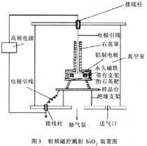
The ion beam sputtering method can control the substrate at a lower temperature range during film formation. It can not only sputter various alloys and refractory metals, but also can sputter an insulating film such as SiO2. The sputtered film has better uniformity, repeatability, and good step coverage, and the sputtered film can be controlled more precisely, which is more advantageous for manufacturing a fine-sized insulating film [9]. However, due to the high voltage and gas used in the sputtering, the instrumentation is more complicated. The formation of nanomaterials is greatly affected by the sputtering atmosphere and the deposition rate is also low. The radio frequency magnetron sputtering technology developed with it can meet both the fast and low temperature requirements. The device structure is shown in Figure 3 [10]. The SiO2 film prepared by radio frequency magnetron sputtering has advantages of compact structure and high purity [10].
Controlled sputter is a sputter coating method that improves the shortcomings of electrons in the cathode sputtering process that cause the substrate temperature to rise too fast, adding a quadrature magnetic field between the sputtered target (anode) and the cathode. The electric field, electric field, and magnetic field are perpendicular to each other. When the coating chamber is evacuated to a set value and filled with an appropriate amount of argon gas, a voltage of several hundred volts is applied between the cathode (column target or planar target) and the anode (coating chamber wall) to generate a magnetic control type in the coating chamber. Abnormal glow discharge, argon is ionized. Under the action of orthogonal electromagnetic fields, electrons travel along the target surface in a cycloid manner. The movement of electrons is confined within a certain space, increasing the collision probability with the working gas molecules, and increasing the ionization efficiency of the electrons. After multiple collisions, electrons lose their energy and become the "final electron" into the weak electric field. At the end of the electron, they are already low-energy electrons and will no longer overheat the substrate. At the same time, the high-density plasma is trapped near the target surface and is not in contact with the substrate. The surface atoms of the target material are sputtered and deposited on the surface of the workpiece to form a thin film. The substrate can be shielded from plasma bombardment and the substrate temperature can be reduced. Different targets and different sputtering times can be controlled to obtain thin films of different materials and thickness [5].
The quality of radio frequency sputtering is influenced by factors such as pre-evacuation degree, argon pressure during sputtering, sputtering power, sputtering time and substrate temperature. In order to obtain an ideal sputter film, these influencing factors must be optimized [11] ]. The nanofilms are obtained mainly through two approaches: (1) controlling the formation of nanostructures during the process of amorphous thin film crystals; (2) controlling the formation of nanostructures during the nucleation and growth of thin films, in which the deposition conditions of thin films are controlled. Extremely important. In the sputtering process, nanostructured thin films can be easily obtained using high sputtering gas pressure and low sputtering [12].
U.S. BGPotter and the Koch team of the Munich University of Technology in Munich used sputter methods to prepare nanocomposite films with nano-semiconductors embedded in dielectric films. Baru et al. used Si and SiO2 combined targets for RF magnetron sputtering to obtain Si/SiO 2 nano-inlaid composite thin film luminescent materials. The sputtered film can be sputtered on any substance in principle, and various nano luminescent materials can be conveniently prepared. It is a widely used method for physically depositing a nano composite film [13].
Researchers at Tohoku University’s School of Engineering also made progress in the preparation of multilayered nanocomposite magnets. They used RF magnetron sputtering to prepare Nd-Fe-B-Fe multilayer films and Nd-Fe-B monolayer films, which were sputtered with Nd13Fe70B17 alloy target. Relevant research has yielded a number of meaningful data [14].
3 Research and Prospects of Nanomaterials in China
China has established a variety of physical and chemical methods for preparing nanomaterials, and developed more than 10 devices for preparing nanomaterials such as gas evaporation, magnetron sputtering, laser-induced CVD, and plasma-heated gas-phase synthesis; and chemical coprecipitates and sols have been developed. Gel, microemulsion hydrothermal, non-aqueous solvent synthesis and supercritical liquid synthesis methods for preparing nanomaterials including metals, alloys, oxides, nitrides, carbides, ion crystals, and semiconductors Size controllable; developed into a variety of excellent performance of a variety of nano-films and blocks. The characterization of nanomaterials, the causes and elimination of agglomerates, the adsorption and desorption of the surface, the preparation of nanocomposite particles and powders have all been innovative, and significant progress has been made. In recent years, a variety of methods have been established and developed for the preparation of nano-structured assembly systems, in particular, self-assembly and molecular self-assembly, template synthesis, carbothermal reduction, droplet epitaxial growth, and mesoporous in-line growth have also accumulated rich experience. , has successfully prepared a variety of quasi-one-dimensional nanomaterials and nano-assembly system. These methods have laid a good foundation for the further study of the physical properties of nanostructures and quasi-one-dimensional nanomaterials, advancing their application in nanostructured devices. The evaluation methods for nanomaterials and nanostructures are basically complete, reaching the international advanced level in the late 1990s [15].
It can be predicted that with the rapid development of nano-science and technology, more and more new types of nano-materials will be widely used, triggering tremendous changes in related industries.
Source: State Key Laboratory of Sensing Technology, Shanghai Institute of Technical Physics, Chinese Academy of Sciences
Household Cleaning Products And Accessories
Household Cleaning Products And Accessories,Cleaning Cloth,Oil Removal Dishwashing Cloth,Thickened Suction Kitchen Artifact
Huayao Master (Puyang) Automation Equipment Co., Ltd. , https://www.huayaolive.com